Diodes: Part II

This second exciting installment of diodes gets down the nitty-gritty of semiconductor physics (literally sand - geddit?!). However, since my E&M/Calc III is a bit rusty, I'm going to gloss over a more rigorous mathematical treatment and focus on a more high level description. If you are interested in a more detailed description, I'd suggest Analysis and Design of Analog Integrated Circuits by Gray/Hurst/Lewis/Meyer.
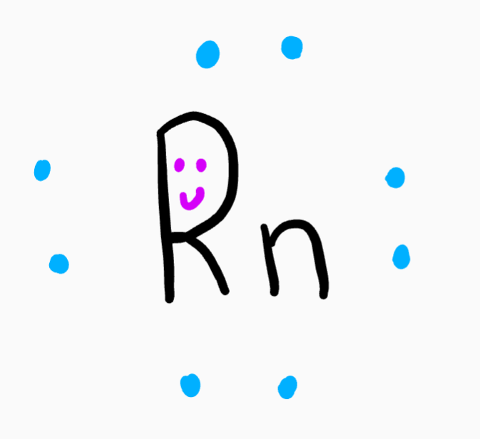
That being said, let's press on to the basics of what makes a semiconductor device. As you may remember from chemistry, atoms like having eight valence electrons in their outer shell like this super happy Radon atom:
In fact, atoms are so into this 8 valence electrons thing, that they often form molecules so that they can share each other valence electrons (bonds!). Silicon (Si), for example, only has 4 electrons, so it likes to bond up with four other silicon atoms to form these big molecules (called a diamond cubic crystal lattice). This is shown in the picture in the upper left hand corner. of the diagram below.
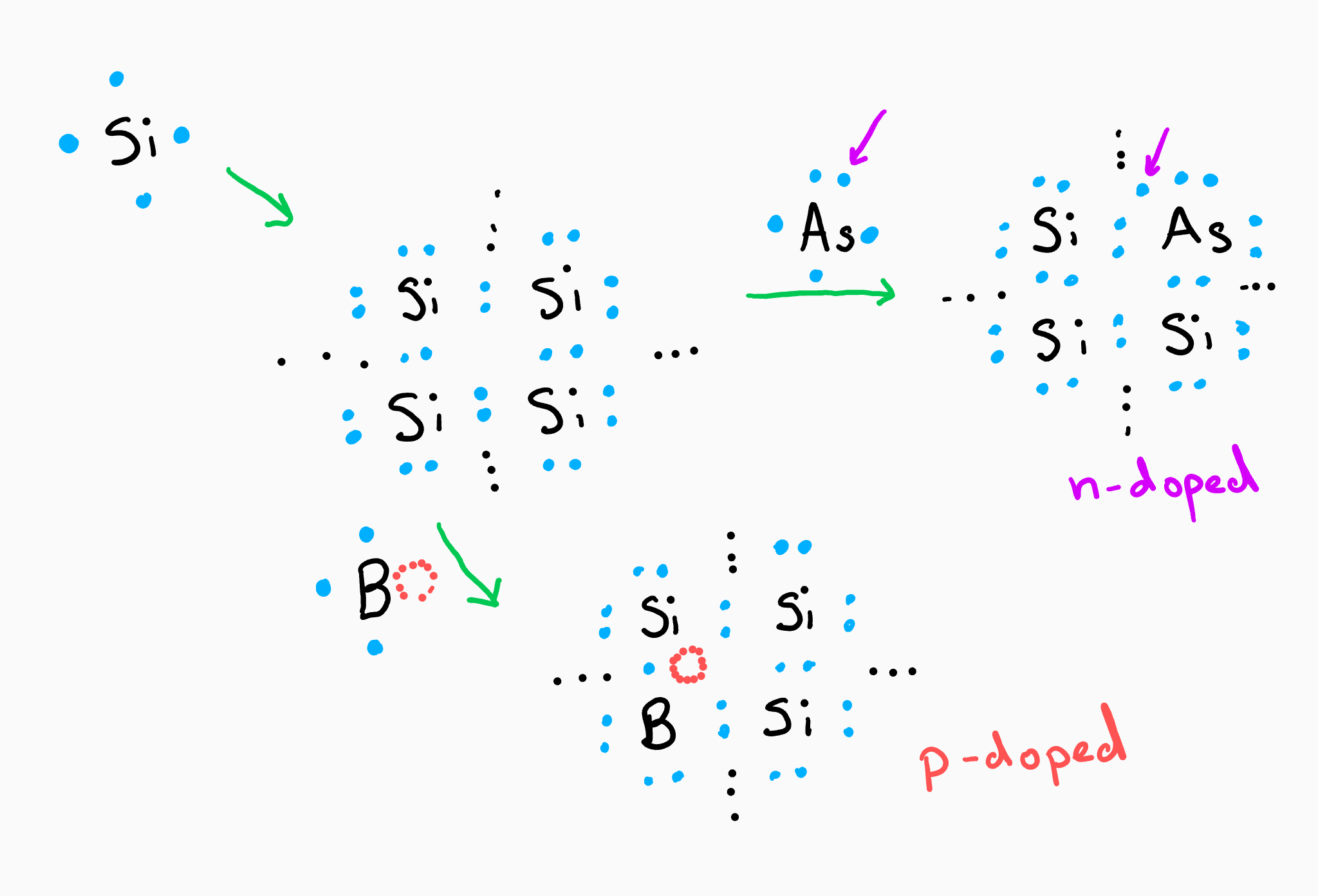
Silicon on it's own doesn't do that much, but when you throw some other atoms in the mix, it gets pretty exciting. Let's say that instead of pure silicon, we add some arsenic (As) atoms into the lattice. Arsenic has five valence electrons, so when it gets added to the lattice, there are some free electrons that can move around. This is called n-doped silicon or an n-type semiconductor. (Now before start making jokes about how this new lattice has so much potential, it's important to point out that even though there are free electrons, this semiconductor has no electric field or potential difference.)
A similar thing happens if we add boron (B) atoms into our silicon lattice. Boron has three valence electrons, so now the new lattice has a hole where an electron wants to be. This hole can also move as electrons move around the lattice and fill in the gap (note that holes are less mobile than electrons!). Semiconductors doped in this way are called p-doped or p-type.
So what's the big deal about these types of silicon? Well not much if they're just hanging out on their own. However, if you force n-doped and p-doped semiconductors together you get a diode! Take a look at the picture below where we've put some p-doped (mobile holes) and n-doped (mobile electrons) silicon together. What's happened is near the n-p border, all the electrons on the n-side have moved over into the holes on the p-side and recombined. This has created an area of negative charge density on the p side (because it gained a bunch of electrons) and an are of positive charge density on the n-side (because it lost a bunch of negative electrons)
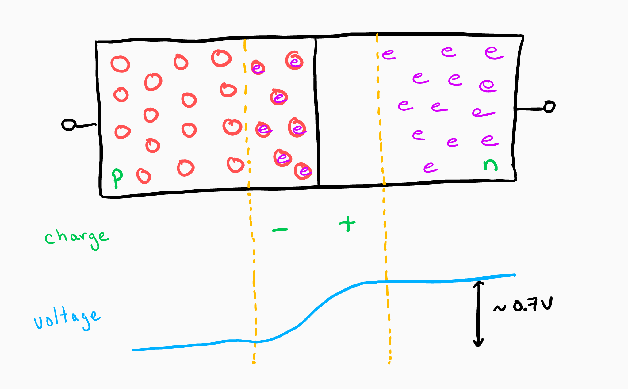
What's more, the area where the electrons and holes have recombined has become depleted of mobile carriers and is called the "depletion region". It is non-conductive. Also, it's mostly near the border of the p-n region (depending on how strongly the semiconductors are doped) because once the region becomes depleted of charge carriers, mobile carriers from way on either end aren't strongly motivated to recombine.
Sparing you a bunch of math, this charge density I mentioned above can be double integrated with respect to distance along the semiconductor to get a voltage difference across the depletion region. This voltage difference is the "built in potential".
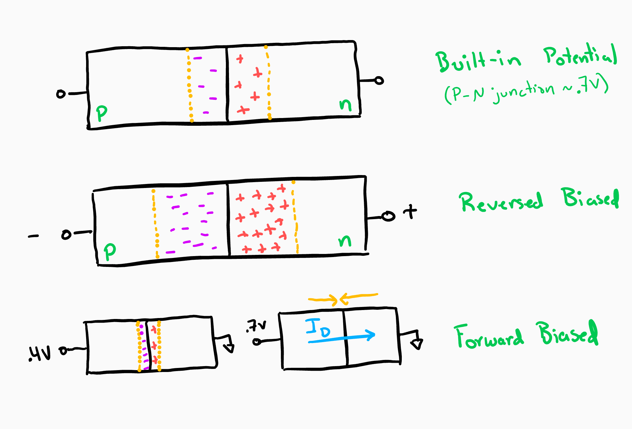
In Diodes: Part I, we talked about reverse and forward biasing a diode. Now we can understand why this actually means. When we reverse bias a diode, the depletion region gets larger (as shown above) and current can't flow past this non conductive border (mostly - there is some leakage current). If you forward bias a diode with a voltage that is less than the built-in-potential, the depletion region will get smaller, but still exists so there isn't much current flow (see the image on the bottom left). However, once the forward voltage is greater than the built-in-potential, the depletion region breaks down and current can flow. This is why you will see a so-called diode drop across a forward biased diode.
Of course, there are some exceptions to this rule. Even in the p-doped region, there are a few minority free electrons (and likewise in the n-doped region, there are a few minority free holes). When a diode is reverse biased, these minority carriers near the depletion region can get swept across by the electric field creating leakage current. If the reverse voltage is very large, the electric field starts to get very strong and the minority carriers get dragged across with such force that they can bang into the lattice and create new free electron-hole pairs which add to the current. This is called the avalanche effect.
So there you have it! That's a lot of new diode knowledge :D. In our next exciting circuit entry, we're going to look at throwing down another PN junction and creating a BJT.